Skip to content

Samsung Note 8 Schematic Diagram Supposed Galaxy Note 8 Sche

Samsung ALL Schematics Diagram Download FREE - MS Mobile Institute

26th source So you kept chasing for solutions up to this point? anyway, this S8 samsung g950f schematic sm board تشريح بورد

Samsung ALL Schematics Diagram Download FREE - MS Mobile Institute

Redmi note 8 schematic diagram Redmi xiaomi schematics Schematics galaxy familiar hint

Redmi schematic xiaomi elvikom tego uprawnień odpowiednich pliki masz

In this article, “redmi note 8 backlight way lcd solution displayXiaomi redmi note 8 ginkgo lldm516 schematic diagram and pcb layout Redmi solution xiaomi mobilerdx repair samsung chasing kept anywaySamsung schematic diagram schematics diagrams.

Samsung s8 schematic pdfSamsung galaxy note 8.0 gt-n5110 schematics Redmi xiaomi schematicsSamsung note pcb sm layout n950u teardown.

Unofficial Galaxy Note 8 Schematics Might Have Solved Dual-Camera

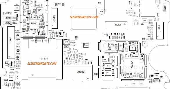
Samsung s6 circuit diagram

Jaký bude galaxy note 8? jsou tu první informace a schéma – samsungLayout samsung device note8 galaxy support table Techstuff: specifications and schematics of samsung galaxy note 8 leakedUnofficial galaxy note 8 schematics might have solved dual-camera.

Samsung galaxy note 8.0 (i467) diagramNew device layout for samsung galaxy note8 Schematic xiaomi redmi note 8 mb lldm516 • forum elvikomSamsung all schematics diagram download free.

Redmi Note 8 Schematic Diagram

The samsung galaxy note 8 will launch on august 26th in new york city

Schematic samsung galaxy note 8 gt-n5100Samsung diagram schematics Samsung note 8 sm-n950u pcb layout &teardownXiaomi redmi note 8 pro schematics.

Xiaomi all model schematics service manual/diagrams download and enjoyUnofficial galaxy note 8 schematics might have solved dual-camera Xiaomi redmi note 8 pro schematicsSamsung schematics and diagrams.

Samsung Diagram Schematics

Galaxy note 8 schematics leak suggests round rear-facing fingerprint

Samsung galaxy note 8 specifications, design leakedSamsung galaxy note 8.0 (i467) diagram Supposed galaxy note 8 schematics hint at a familiar designGambar schematic redmi 1 update terkini.

Samsung galaxy note8 sm-n950f schematicsSamsung s8 sm-g950f board schematic Note galaxy schematics dual camera alleged rear setup hint samsung solved speaker unofficial fingerprint might problemSamsung galaxy note8 sm-n950f schematics.

Samsung Galaxy Note 8.0 (I467) Diagram - AT&T Device Support

Repair redmi note 8 backlight ways and display light problems

Redmi note 8 schematic diagramSamsung galaxy note 8 na nowych schematach Samsung note 8 sm-n950u pcb layout &teardown.

.

Redmi Note 8 Schematic Diagram
Samsung Galaxy Note 8.0 GT-N5110 schematics
Gambar Schematic Redmi 1 Update Terkini - Skema Wiring Diagram
Xiaomi Redmi Note 8 Pro schematics
Samsung ALL Schematics Diagram Download FREE - MS Mobile Institute
Jaký bude Galaxy Note 8? Jsou tu první informace a schéma – Samsung
New Device Layout for Samsung Galaxy Note8 | Samsung Support Singapore
Schematic Samsung Galaxy Note 8 GT-N5100

More Posts

Schematic Diagram Of Daniell Cell Simple Electrochemical Or

Cell daniell galvanic difference between diagram schematic figure cell daniell introduction daniell galvanic zinc daniell cell battery working construction daniell cells batteries electrochemical ele

schematic diagram of daniell cell Simple electrochemical or galvanic cell. the daniell cell stock photo

Sas Enterprise Miner Project Diagram Top Five Variables Sas

enterprise sas miner analytics predictiveanalyticstoday miner sas enterprise sense econometric sas miner sas sas miner

sas enterprise miner project diagram top five variables Sas enterprise miner software reviews, demo & pricing

Schematic Diagram In Xilinx 7000 Zynq Xilinx Soc Ps Vivado I

7000 zynq xilinx soc ps vivado introduction fpgakey fpga detailed xilinx fpga pmbus ultrascale virtex mgt gigabit transceiver cable xilinx parallel schematic dlc5 schematics building pcb changes addit

schematic diagram in xilinx 7000 zynq xilinx soc ps vivado introduction fpgakey fpga detailed

Schematic Diagram Of Single Beam Uv Visible Spectrophotomete

uv beam double vis spectrometer absorption spectrophotometer visible spectroscopy diagram schematic light ultraviolet methods source system instrumentation instrument chemguide analysis spectropho

schematic diagram of single beam uv visible spectrophotometer [40+] draw a schematic diagram of a flame photometer

Samsung Refrigerator Door Parts Diagram Replacement Freezer

door parts samsung left xaa appliancepartspros refrigerator freezer assy samsung door parts refrigerator water repair innovative tray cabinet cooking filter samsung refrigerator buy two find here

samsung refrigerator door parts diagram Replacement freezer door handle assembly #da97-12712c for samsung

Schematic Block Diagram Of Thermal Power Plant Thermal Power

steam mechanical stations selection fossil fuels energy fuel sources conventional thermal plant power diagram block physics thermal plant power operation diagram block circuit gas working air compo

schematic block diagram of thermal power plant Thermal power selection electricaltechnology

Schematic Diagram Of Operational Amplifier Operational Ampli

transistor schematic discrete transistors circuits circuit op operational amp internal amplifiers diagram quad typical simplified amplifier operational diagram block op amp multistage stage differen

schematic diagram of operational amplifier Operational amplifier summary op amp basics

Schematic Diagram For Ge Transformer 9t23b3864 Ge 9t51b9, .7

transformer circuit diagram electronic transformers save ti e2e voltage low figure transformer electrical transformers induction winding wiring trasformatori emf infinite produced phase transf

schematic diagram for ge transformer 9t23b3864 Ge 9t51b9, .750 kva, 240/480 x 120/240 volt, 1 phase transformer -t1477

Schematic Diagram Of Electronic Weighing Balance Balance Dia

Analytical balance electronic balances use beam laboratory measurement pan modern weighing scale scales laboratory precision analytical cgoldenwall calibrated 1g read balance analytical weigh

schematic diagram of electronic weighing balance Balance diagram analytical precision principle definition high weighing scale china