Samsung G530 Schematic Diagram Agus: [34+] Samsung G532f Sch
Jumper samsung j2 g532f jalur charging schematic diagrama solution patah g530 cas hp clangsm circuito mesin network charger reparo mic Samsung galaxy grand prime g530 diagram [diagram] samsung g530 diagram
Schematic Diagram
Schematic diagram Samsung galaxy a52 5g sm-a526b schematics Samsung g530,g531,g532 lcd light solution
[diagram] samsung g530 diagram
Samsung gt s5830i circuit diagramSamsung sm-g530h lcd display ic solution jumper problem ways ~ gsmsony Schematics samsung galaxy grand prime sm-g531fGrand skematik.
Samsung galaxy g530 power ic replacementSchematic samsung g532f [view 31+] samsung g532 schematic diagramSchematic diagram samsung g532g.
![[DIAGRAM] Lenovo T530 Diagram - MYDIAGRAM.ONLINE](https://i2.wp.com/www.laptopschematic.com/wp-content/uploads/2012/02/Samsung-N150-Block-Diagram.png)
G531f schematics
Samsung g532 light lcd g530 solution g531[view 34+] samsung g532f schematic diagram [diagram] lenovo t530 diagramSamsung j510f schematic diagram.
Samsung galaxy g530 lcd light solution[diagram] samsung g530 diagram Diagram samsung prime grand galaxy g530Download samsung galaxy a53 5g schematic diagram.

Samsung clone g530f-g530h-g530 flash file
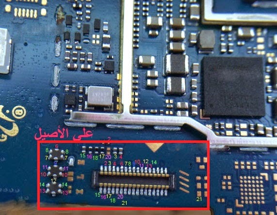
Charging g530h mobilerdxشماتیک samsung t530 schematic بصورت کامل G530h samsung clone g530 flash file mt6572 smSamsung g530 lcd solution light galaxy.
[diagram] samsung g532g diagramG532f galaxy prime agus smartphone Samsung g530h charging waysLenovo ideapad s530-13iwl schematic la-g651p elz02 motherboard – laptop.
Galaxy note 2 schematic diagram
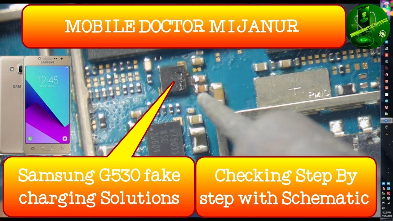
Samsung g530h display lcd jumper sm solution ic problem ways board diagramUpdate_layout_samsung galaxy a53(sm-a536b)_bitmap Samsung g530 fake charging solutions by schematicSkematik samsung sm-g530g (galaxy grand prime).
Agus: [34+] samsung g532f schematic diagram downloadSamsung_g530h_emmc-pinouts Samsung schematic diagram[diagram] samsung g530 diagram.

Lg g5300 schematics. www.s manuals.com. schematics
Sm g530/g532 lcd ori – cme distribution sdn bhdSmartphone printed circuit board components .
.


![[View 34+] Samsung G532f Schematic Diagram](https://i2.wp.com/phonelumi.com/wp-content/uploads/2016/01/samsung-galaxy-s5-schema.jpg)


![[View 31+] Samsung G532 Schematic Diagram](https://i.ytimg.com/vi/5L0QqMmPZJA/maxresdefault.jpg)